Table Of Content
They provide a compact and organized layout for components, reducing the overall size of the device. PCBs also offer improved reliability and durability, as the connections between components are more stable compared to manual wiring. Additionally, PCBs allow for easier troubleshooting and repair, as faulty components can be easily identified and replaced. High-density interconnect (HDI) PCBs feature fine pitch traces, small vias, and high component density, making them crucial for the increasing miniaturization and functionality demands of modern electronics. These boards are indispensable in applications requiring high-speed data transfer, such as 5G networks, high-performance computing, and advanced driver assistance systems (ADAS) in vehicles.
Ensure a Clear PCB Return Current Path
These choices are important because they affect the trace width you can use in the circuit board design; different routing styles will enforce different trace widths in order to hit your required impedance. If you’re working on a high speed/high frequency circuit board design, you can use the built-in impedance profiler to ensure impedance control in your board. The impedance profile tool uses an integrated electromagnetic field solver from Simberian to tailor the geometry of your traces to meet a target impedance value. If the printed circuit board shape, dimensions, and layer stackup for your board have already been determined, you can set them now.
Step 1: Schematic Capture
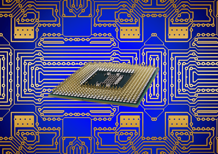
A PCB trace is a thin copper line etched onto a printed circuit board (PCB) that serves as a conductive pathway between different components on the board. PCB designers must carefully consider the layout and routing of traces to ensure that the circuit functions correctly and reliably. A printed circuit board (PCB) is a fundamental component of electronic devices that provides a platform for the assembly and connection of various electronic components.
IPC-22XX 1.X. Definition for Printed Circuit Engineering Layout Professional
It is a flat board made of non-conductive material, usually fiberglass, which is then coated with a layer of conductive material like copper. The conductive material is etched into specific patterns, creating a network of pathways or traces. The primary purpose of a PCB is to provide mechanical support and electrical connections for electronic components such as resistors, capacitors, diodes, and integrated circuits. These components are soldered onto the surface of the PCB, and the traces on the board allow for the flow of electric current between them.
UHDI Fundamentals: Ultra HDI Pushes PCB Manufacturing Capabilities - I-Connect007
UHDI Fundamentals: Ultra HDI Pushes PCB Manufacturing Capabilities.
Posted: Thu, 26 Oct 2023 07:00:00 GMT [source]
These boards consist of conductive tracks, pads, and other features etched from copper sheets laminated onto a non-conductive substrate, such as FR-4. PCBs are crucial in various applications, from consumer electronics to industrial equipment and aerospace systems. The different types of printed circuit boards, including single-sided, double-sided, and multi-layer boards, cater to specific design requirements and constraints.
While many of the previous components on the list are used to transfer electrical current in some form or another, capacitors do the opposite. Like batteries, they are used to store electrical charge or harbor electrical current. However, where a battery stores electrical energy, capacitors store electrical energy. A capacitor is made from two or more metal plates that sandwich a dielectric between them. Aside from the battery, possibly the second most common component — at least when it comes to hobby projects — is a light-emitting diode, or LED. LEDs simply take the charge or current from the battery or the capacitor, which is then used to power the light portion of the LED.
In the past, electronics were designed and assembled from small integrated circuits (ICs) and discrete components, which were connected together using wires, and the components were mounted to a rigid substrate. This original substrate was initially a material called bakelite, which was used to replace the top ply on a sheet of plywood. The number of wires was so great that they could get tangled or inhabit a large space within a design. Manufacturing was also slow, where multiple components and their wired connections were manually soldered.
PCB Layout Basics Part 1: Getting Started with Circuit Board Design Software
Engineers meticulously analyze the circuit’s requirements and constraints to ensure optimal performance and reliability. This visual representation of the circuit illustrates the connections between components. There are things multi-layer boards can do that single and even double-layer boards can’t even come close to.

Source Data Fig. 3
TTM Technologies, Inc. operates another facility in Forest Grove, OR, with 580 employees. This manufacturer designs PCBs for the computing and medical sectors, just to mention a few. Once a path through the circuit is created, the charges in the capacitor can find another way to each other — they don’t have to keep trying to go through the dielectric.
Altium Designer will treat your custom design rules just like the built-in design rules. As you place components, vias, drill holes, and traces, the unified design engine in Altium Designer will automatically check the layout against these rules and will flag you visually if there is a violation. The last point above is quite important, as complex designs may use hierarchical schematics. You can enforce significant organization in your new board if you take a hierarchical approach to your circuit board design and place different circuit blocks in different schematics. Finally, a few words on the utility of designing your own circuit boards. It also allows you to sell your design if it turns out to be popular.
If necessary, you can create new circuit board design rules by following the steps of Altium Designer’s Design Rule Wizard. When designing a circuit board it may sometimes seem as though arriving at the final design is going to be a long and arduous journey. The next stage involves creating a schematic diagram, which is a visual representation of the circuit. This diagram shows how the components are connected and allows the designer to identify any potential issues or conflicts.
Multi-layer PCBs allow for intricate routing, better signal integrity, and improved thermal management, as the inner layers can be used for power and ground planes. The increased number of layers also enables the use of advanced techniques, such as blind and buried vias, which further enhance the capabilities of multi-layer PCBs. However, the increased complexity and manufacturing requirements of multi-layer PCBs are more expensive than single-sided and double-sided boards.
Design for Assembly (DFA) is a complementary concept to DFM, focusing specifically on optimizing the assembly process. DFA aims to simplify and streamline the assembly of the PCB by reducing the number of assembly steps, minimizing the risk of errors, and enhancing overall productivity. Usually, each active component on the board (ICs and other related components) need to be connected to power and ground nets. This is easily accomplished by flooding areas or layers with solid planes that these components can tap into.
The purpose of schematic design is to create a graphical representation of the electrical connections and components in the circuit, using standardized symbols and notations. The first step in the PCB design workflow is the conceptual design phase, where the overall requirements and specifications of the electronic product are defined. Sensitive analog components, high-speed digital components, and power supply circuitry should be placed in a way that minimizes crosstalk, noise, and electromagnetic interference (EMI). When designing a circuit board layout, you also need to consider the space offered to you overall. You should know how much space you have based on the detailed schematics made in the earlier section.
The traces are the flat wires connecting your PCB together and need to be controlled in terms of width and thickness. This then ensures power is distributed equally, and no concerns are surrounding the voltage of the PCB. We have only scratched the surface of what is possible to do with Altium Designer on Altium 365. You can check the product page for a more in-depth feature description or one of the On-Demand Webinars.
Before routing your traces, it is a good idea to place your drill holes (mounting and vias). If your circuit board design is complicated you may need to modify at least some of the via locations during trace routing. Make sure you decide your routing style before you start calculating impedances. For example, will you be using a coplanar line on a thicker dielectric layer, such as in this example, or will you be using a standard microstrip/stripline on a thinner dielectric?


No comments:
Post a Comment